
Natural and commercial materials Tradescantia spathacea leaves were obtained from potted plants in our office. PVC foam boards (PVC-Schaumplatte Fixmaß, Bauhaus AG, 250 × 500 × 3 mm3) and transparent PS glass (Hobbyglas Owocor, Bauhaus AG, 250 × 500 × 2 mm3) were purchased from a local hardware store. Fluorinated ethylene propylene (FEP) film (Nenull, 140 × 200 × 0.15 mm3), copper foil tape (3M 1181 Kupferband leitend, 0.04 mm, 50 mm × 16.5 m),
Natural and commercial materials
Tradescantia spathacea leaves were obtained from potted plants in our office. PVC foam boards (PVC-Schaumplatte Fixmaß, Bauhaus AG, 250 × 500 × 3 mm3) and transparent PS glass (Hobbyglas Owocor, Bauhaus AG, 250 × 500 × 2 mm3) were purchased from a local hardware store. Fluorinated ethylene propylene (FEP) film (Nenull, 140 × 200 × 0.15 mm3), copper foil tape (3M 1181 Kupferband leitend, 0.04 mm, 50 mm × 16.5 m), super-hydrophobic spray (Glaco Mirror Coat Zero, 40 ml) and PS sheets (Evergreen Scale Models, 130 μm) were purchased from an online shop.
Sample preparation
Sixteen sample types were prepared:
-
(1)
PFOTS layers on quartz. Quartz plates (75 × 25 × 1 mm3, proQuarz GmbH) were treated with O2 plasma at 300 W for 10 min (Femto low-pressure plasma system, Diener electronic). Using CVD, 1H,1H,2H,2H-PFOTS (97%; Sigma-Aldrich) was then coated on the surface of the quartz plate. The cleaned quartz plates were subsequently placed in a vacuum glass container together with a vial containing 0.5 ml PFOTS. Then we evacuated the container to a pressure below 100 mbar, closed the pump and let it react for about 30 min. Finally, the quartz plates were rinsed with ethanol to remove any unbound silane molecules.
-
(2)
PFOTS layers on ITO glass. ITO glass (75 × 25 × 1.1 mm3, surface resistivity 30–60 Ω sq−1, Sigma-Aldrich) were treated with O2 plasma at 300 W for 10 min (Femto low-pressure plasma system, Diener electronic). Using CVD, 1H,1H,2H,2H-PFOTS (97%; Sigma-Aldrich) was then coated on the surface of the ITO glass. The cleaned ITO glass was subsequently placed in a vacuum glass container together with a vial containing 0.5 ml PFOTS. Then we evacuated the container to a pressure below 100 mbar, closed the pump and let it react for about 30 min. Finally, the ITO glass was rinsed with ethanol to remove any unbound silane molecules.
-
(3)
60-nm Teflon-coated copper. To obtain flat copper substrates, a 35-nm-thick copper layer was sputtered onto a quartz plate. A 60-nm-thick Teflon film was then coated onto the copper by dip-coating with a pulling speed of 10 mm min−1 from 1 wt% Teflon AF 1600 (εr = 1.9, Sigma-Aldrich) in FC-75 (97%, Fisher Scientific). Finally, the Teflon-coated copper samples were heated in an oven at 160 °C under vacuum for 24 h. The film thickness was measured by a profiler (P-7 stylus profiler, KLA-Tencor).
-
(4)
A 60-nm-thick PS film was coated onto the copper by dip-coating with a pulling speed of 60 mm min−1 from 2 wt% PS (molecular weight 192 kg mol−1, εr = 2.6; Sigma-Aldrich) in toluene (99.8%, Sigma-Aldrich). The sample was then heated in an oven at 120 °C under vacuum for 24 h.
-
(5)
A 200-nm-thick PS film was coated onto copper by dip-coating with a pulling speed of 40 mm min−1 from 4 wt% PS in toluene. The samples were then annealed (120 °C under vacuum for 24 h).
-
(6)
A 1-μm-thick PS film was coated onto copper by dip-coating with a pulling speed of 20 mm min−1 from 10 wt% PS in toluene. The samples were then annealed (120 °C under vacuum for 24 h).
-
(7)
A 5-μm-thick PS film was coated onto copper by dip-coating with a pulling speed of 10 mm min−1 from 20 wt% PS in toluene. The samples were then annealed (120 °C under vacuum for 24 h).
-
(8)
200-nm PS-coated gold samples. A 35-nm gold layer was sputtered onto quartz plates. A 200-nm PS film was then coated onto the gold layer by dip-coating, as described previously.
-
(9)
60-nm SiO2-coated gold samples. First, a 35-nm gold layer was sputtered onto quartz plates. Then a 60-nm SiO2 layer was sputtered onto a gold layer.
-
(10)
60-nm Teflon-coated aluminium sample. First, a 100-nm aluminium layer was deposited onto glass slides (76.2 × 25.4 × 1 mm3, Sail Brand) by vacuum thermal evaporation. Then a 60-nm Teflon film was coated on the aluminium layer by dip-coating with a pulling speed of 10 mm min−1 from a solution of 1 wt% Teflon AF 1600 (εr = 1.9, Sigma-Aldrich) in FC-75 (97%, Fisher Scientific). Finally, the samples were annealed (160 °C under vacuum for 24 h).
-
(11)
PFOTS layers on aluminium. First, a 100-nm aluminium layer was deposited onto glass slides. The sample was then treated with O2 plasma at 300 W for 10 min and PFOTS was deposited by CVD, as described previously.
-
(12)
60-nm Teflon-coated quartz–copper samples (for sliding experiments). We used a rectangular mask to cover two-thirds of the quartz plate (75 × 25 × 1 mm3, proQuarz GmbH) and 35 nm of copper was sputtered onto the uncovered area. After removing the mask, we obtained a plate with one-third covered by Cu and two-thirds comprising the quartz surface. The boundary between the quartz and copper areas formed a sharp straight line. Finally, a 60-nm Teflon film was coated on this plate by dip-coating with a pulling speed of 10 mm min−1 from 1 wt% Teflon AF 1600 (εr = 1.9, Sigma-Aldrich) in FC-75 (97%, Fisher Scientific). Finally, the samples were annealed (160 °C under vacuum for 24 h).
-
(13)
200-nm PS-coated quartz–gold samples (for sliding experiments). We used the same method as above to make a substrate of two-thirds quartz and one-third 35-nm gold. A 200-nm PS film was then coated on this plate by dip-coating with a pulling speed of 40 mm min−1 from 4 wt% PS in toluene. Then the samples were annealed (120 °C under vacuum for 24 h).
-
(14)
60-nm Teflon-coated commercial copper foil samples. A 40-μm-thick single-sided copper foil tape (3M 1181 Kupferband leitend, 0.04 mm, 50 mm × 16.5 m) was cut into dimensions of 50 mm × 25 mm, stacked face to face on the adhesive side and cleaned with ethanol. A 60-nm-thick Teflon film was then coated onto the copper by dip-coating with a pulling speed of 10 mm min−1 from 1 wt% Teflon AF 1600 (εr = 1.9, Sigma-Aldrich) in FC-75 (97%, Fisher Scientific). Finally, the samples were heated in an oven at 160 °C under vacuum for 24 h.
-
(15)
500-nm super-hydrophobic coating commercial Copper foil samples. A 40-μm-thick single-sided copper foil tape (3M 1181 Kupferband leitend, 0.04 mm, 50 mm × 16.5 m) was cut into dimensions of 50 mm × 25 mm, stacked face to face on the adhesive side and cleaned with ethanol. A commercial super-hydrophobic spray (Glaco Mirror Coat Zero) was applied to copper foil from a distance of approximately 0.5 m for 3–4 s. The sample was then left undisturbed for 30 min to allow the ethanol in the solution to evaporate.
-
(16)
A 12-μm-thick PS film was coated onto copper by dip-coating with a pulling speed of 10 mm min−1 from 30 wt% PS in toluene. The samples were then annealed (120 °C under vacuum for 24 h).
Water drop impact experiments
We generated water drops with a volume of 35 μl water (<1 μS cm−1; Gibco, Thermo Fisher Scientific) containing 1 mM NaCl (diluted from 1 M NaCl solution, Carl Roth) through a grounded syringe needle (electrically neutral). The needle was connected to a peristaltic pump (MINIPULS 3, Gilson). Water drops were released from a height of about 4 cm from the sample surface at intervals of 12 s. More than 1,000 water drops were continuously released in each experiment. The sample was tilted by 10° so that, after impact, the water drop rolled off the surface. Each water drop always showed the same behaviour (Supplementary Fig. 19).
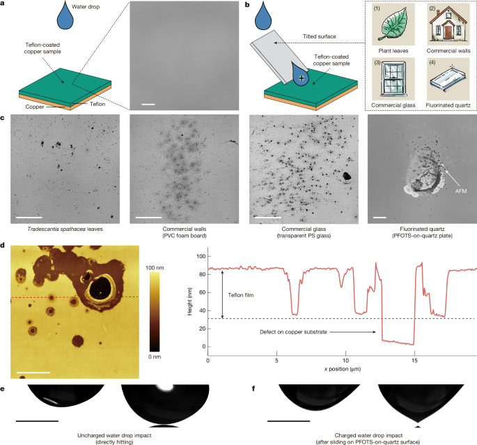
In the experiments of the spontaneously charged water drops that induce corrosion, the water drops first fell onto the top of a 50° tilted surface (Tradescantia spathacea leaves, PVC foam board, PS glass, FEP film or PFOTS-on-quartz plate) at intervals of 12 s from a release height of about 5 mm. Driven by gravity, water drops slid down roughly 4 cm and then left the tilted surface. During this process, the water drops undergo slide electrification, causing them to accumulate charge and deposit opposite charge onto the tilted surface. To achieve defined electrical conditions, the tilted surfaces were placed on a grounded metal plate. After the water drops left the tilted surface, they carried the electrical charge and, after falling about 5 mm, hit the Teflon-coated copper or other samples. A similar discharge cone was observed at different falling heights (Supplementary Fig. 20). As well as the 1 mM NaCl, there were more salt solutions (10 mM NaCl (Carl Roth), 100 mM NaCl (Carl Roth), 10 mM KCl (Carl Roth), 10 mM NaBr (Carl Roth), 10 mM KNO3 (Carl Roth), 10 mM ZnSO4 (Fluka) and also deionized water (<1 μS cm−1; Gibco, Thermo Fisher Scientific) and rainwater collected from the Mainz area.
The charge deposited by the drops on the tilted surface reduced the slide electrification effect of subsequent drops. Because it takes several minutes or more for the surface to naturally return to electrical neutrality, we needed to speed up the experimental process. To do this, we used an ionizing air blower (Aerostat PC ionizing air blower, Simco-Ion), which continuously neutralized the charge on the tilted surfaces during the experiment. This ensured that each subsequent water drop had the same slide electrification effect. In practice, tilted surfaces were neutralized in the 12 s between subsequent drops. Similarly, more than 1,000 water drops were continuously released in each experiment. Surface neutralization created by the ionized air took several seconds and was negligible while drops were sliding (about 100 ms) but effective in the intervals between drops. We also tested the case without the ionizing air blower and still observed surface corrosion (Supplementary Fig. 21).
For both experiments, we used a side-view high-speed camera (Photron, FASTCAM MINI UX100, 25,000 fps, resolution 1,280 × 200, with 1× SilverTL Telecentric Lens, Edmund Optics) to observe the behaviour of water drops when they hit the Teflon-coated copper surface. For the experiment observing the evolution of surface corrosion patterns from the bottom in situ, we used a non-high-speed camera (FLIR Blackfly S) for recording.
Water drop sliding experiments
The samples for the sliding experiments were placed on a grounded metal plate tilted at 50°. 35 μl water drops containing 1 mM NaCl were released onto the top of a tilted sample from a grounded syringe needle at intervals of 12 s, with a release height of about 5 mm. We used a peristaltic pump (MINIPULS 3, Gilson) to continuously deliver solution from the tank to the syringe. During the experiment, the ionizing air blower (Aerostat PC ionizing air blower, Simco-Ion) was always turned on. In each experiment, about 3,000 water drops were released continuously. We used a bottom-view high-speed camera (Photron, Phantom TMX 7510, 40,000 fps, resolution 1,280 × 800, with 10× UPlanSApo Microscope Objective, Olympus) to observe the behaviour of the water drops when they slid down tilted samples.
Confocal laser scanning microscopy imaging
Surface morphology and fluorescent properties of samples were imaged using a confocal microscope (LSM 880, Carl Zeiss) equipped with a Zeiss Plan-Apochromat 10×/0.45 objective. An argon-ion laser (λ = 488 nm) coupled with an optical fibre to the microscope was used for excitation. The confocal observation volume was positioned on the surfaces studied. Images were recorded either in reflection or in fluorescence mode using an appropriate dichroic mirror and a spectral detection unit (Quasar, Carl Zeiss). This unit comprises a diffraction grating and a 32-channel GaAsP multianode photomultiplier array detector. While recording the fluorescence images, the maximum spectral range of the detected emission light was 517–696 nm. The emission spectra were recorded using the so-called lambda mode of the instrument. In this mode, the spectral range of 520–690 nm was distributed between the 32 channels and the signal in every channel was detected separately. The 3D image of the surface morphology (Supplementary Figs. 15 and 23) was obtained by another confocal microscope (confocal white light microscope, µsurf, NanoFocus AG) equipped with a 20×/0.46 objective, using point-by-point line scanning laser profilometry.
Charge measurements
Charge measurements were conducted using a current amplifier (response time: 0.8 ms, FEMTO DDPCA-300). We recorded the current signal of water drops or metal substrates during impact using a National Instruments data acquisition board (USB-6366 X Series).
Measurement of water drops: the current amplifier was connected to wires with a diameter of 0.7 mm made of tungsten serving as electrodes. The tungsten wire was coated with a layer of gold to enhance electrical conductivity. We measured the current of drops after sliding 4 cm on the surface (Extended Data Figs. 1 and 5a). Also, we measured the current of drops bouncing off the surface (Extended Data Fig. 5c). In both cases, the water drops touched the electrode and caused a current flow. The contact to the wire electrode corresponds to 0 ms (t0) and the drop discharged until t1. After t1, there is a low positive current of about 10 nA until the rear of the drop detaches from the electrode after roughly 20 ms. This low positive current is the result of the continued deposition of negative charge on the surface as the drop moves while still in contact with the electrode. For all samples except for the Tradescantia spathacea leaves, t1 was typically 2 ms. For the leaves, t1 was about 10 ms. The integral of the current from t0 to t1 is the amount of charge generated by slide electrification. We also measured the drop current and charge under different salt concentrations, release intervals and natural rainwater (Supplementary Figs. 4, 21 and 22).
Measurement of the current of metal substrates: here the current amplifier was connected directly to the metal layer. When the water drop hit the surface, a current signal was detected as well (Extended Data Fig. 5b). The contact of the drop onto the surface corresponded to 0 ms and the drop discharged until t1, which was about 2 ms. The integral of the current from t0 to t1 is the amount of charge transferred from the water drop to the metal.
AFM and AFM-IR measurements
Details of the surface morphology were studied using AFM (Dimension Icon, Bruker) in tapping mode. The developed surfaces were uniform and smooth (Supplementary Figs. 23 and 24). Commercial Cu foil had a rough surface and its roughness was slightly reduced after coating with a Teflon film (Supplementary Fig. 25). The cantilever had a nominal resonance frequency of 300 kHz and a spring constant of 26 N m−1 (OTESPA, OPUS). The scan sizes were 0.5 × 0.5, 20 × 20 or 50 × 50 μm2.
The products resulting from dielectric breakdown on the PS film were measured using an AFM-based nano-IR method (Vista One, Molecular Vista). The nano-IR response was recorded in photo-induced force microscopy (PiFM) mode. To obtain images of the surface topography, we excited the second eigenmode of the cantilever resonance frequency and kept the oscillation amplitude constant, using an electronic feedback circuit. The first eigenmode of the cantilever resonance frequency was used to record the nano-IR response. The incident IR light was modulated using the difference frequency between the first and second eigenmodes of the cantilever. This difference frequency was tuned to a maximum response amplitude at the first eigenmode.
SEM-EDS measurements
The determinations by SEM were performed with a HITACHI SU8000 (Hitachi High-Technologies Europe GmbH). The scanning electron microscope was coupled to an XFlash 5010 detector, an X-ray detector that allows simultaneous EDS-based elemental analyses.
Raman measurements
Raman measurements were performed using a WITec confocal Raman spectrometer (alpha300 R, 10× objective, 600/1,200 grooves mm−1 grating, 5 mW) with a 532-nm excitation and 120 s integration. The pristine copper foil was included as a reference sample (Supplementary Fig. 26a).
XRD measurements
XRD measurements were performed using a Rigaku SmartLab diffractometer with a rotating Cu anode (8 keV, λ = 1.5406 Å), a Kβ filter and a HyPix-3000 detector. The sample was placed on a rotating sample stage and measured in θ–θ geometry in the range 10° < 2θ < 80° at a rate of 1° min−1. The X-ray beam has a width of 1 mm. The pristine copper foil was included as a reference sample (Supplementary Fig. 26b).
EIS measurements
EIS was carried out using a Metrohm Autolab N series potentiostat (Autolab PGSTAT204) in a three-electrode configuration. Samples were mounted horizontally in a flat-cell configuration, with the exposed working area defined by an O-ring of diameter 6 mm. An Ag/AgCl electrode (3 M KCl) and a platinum wire were used as the reference and counter electrodes, respectively. The electrolyte was either 10 mM or 600 mM aqueous NaCl and measurements were performed in air at ambient temperature. Impedance spectra were recorded at open-circuit potential over a frequency range of 105 Hz to 0.1 Hz using a sinusoidal perturbation of 10 mV. For 5-μm PS films, the perturbation amplitude was increased to 20 mV to improve the signal-to-noise ratio for these highly resistive samples. The EIS results demonstrated that the developed coatings greatly increase the interfacial resistance, indicating their excellent barrier properties (Supplementary Information Discussion 4). We also used a digital multimeter to test the barrier properties of the coating (Supplementary Fig. 28).
Keep following us for the latest insights.